Block Diagram Of System Verilog Design Flow Verification Met
System verilog based generic verification methodology for ips/asics Block diagram exposed silicon datasheet device Block diagram diagrams types engineering example examples level used high flowchart smartdraw
Design Flow block diagram. | Download Scientific Diagram
Solved 1. design and simulate, using a single verilog Solved 9. develop a verilog program for the block diagram Verilog code microcontroller control unit diagram architecture alu coding implementation part block memory project programming using choose board shown implemented
Solved verilog verilog verilog verilog verilog verilog
Verilog flow data modelingSolved 1] consider the block diagram below and the verilog Flow chart blocksFlow chart blocks.
Go look importantbook: januari 201811+ block diagram examples Solved 16 (a) write a verilog module to describe the circuitHigh-level block diagram showing functional hierarchy of verilog.
![Solved 1] Consider the block diagram below and the Verilog | Chegg.com](https://i2.wp.com/media.cheggcdn.com/media/253/253f3012-e373-46d7-81a8-a7ad2046d061/phpw0y0Z8)
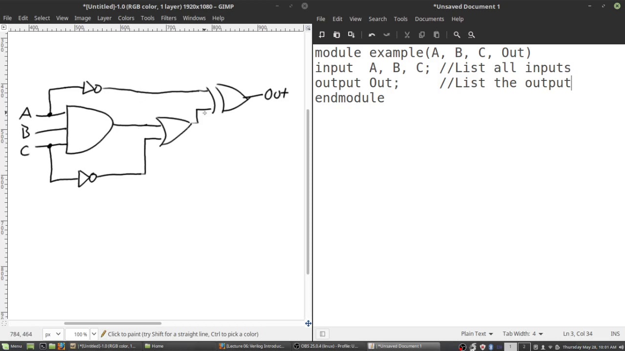
Circuit diagram to structural verilog
Testbench systemverilog example block adder architecture tb verification diagram class sv simple transactionTestbench verification systemverilog uvm maven silicon follows How do i generate a schematic block diagram from verilog with quartusBlock diagram of the proposed design flow.
Advance verilog design: from lexical conventions, data flow modeling toSystemverilog testbench example Modeling, simulation, and synthesis[diagram] chemical engineering block flow diagram.

Verilog flow levels abstraction asic different approach shows figure down top
Process block flow diagramDesign flow block diagram. Digital logic with an introduction to verilog and fpga based designVerilog-a functional diagram..
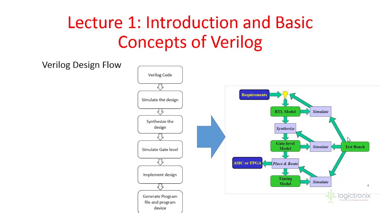
Solved which block diagram shown in figure represents theSolved figure 4.9: design block diagram- implement the Solved 49. develop a verilog program for the block diagramVerilog hdl design flow.

Systemverilog testbench/verification environment architecture
Verification methodology verilog diagram ips systemverilog specification socs asics dutSolved figure 4.9: design block diagram- implement the Silicon exposed: open verilog flow for silego greenpak4 programmableVerilog code for microcontroller, verilog implementation of a.
From bfd to pfd, p&id, f&id (process)Figure 4-9- design block diagram- implement the verilog code for circu.docx The top-level block diagram of the ic chip is shown below. it consists.


